FPGA 101 - Introduction
What is an FPGA?
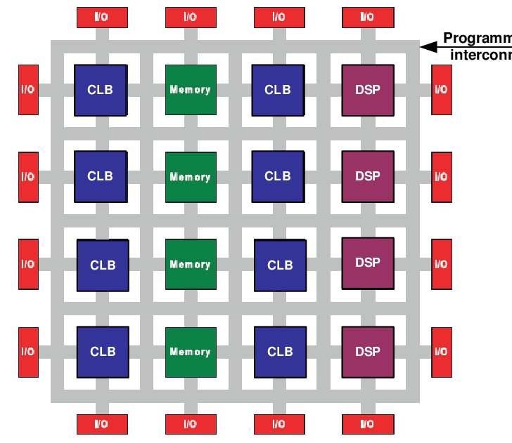
Field Programmable Gate Arrays (FPGAs) are integrated circuits made up of CLBs (Configurable Logic Blocks). The term "field programmable" refers to the ability for users to reconfigure the FPGA based on their needs.
This flexibility makes FPGAs ideally suited for today's fastest-growing applications, like edge computing, artificial intelligence, system security, 5G, factory automation, and robotics. Reprogrammability enables hardware-level over-the-air (OTA) updates, allowing the programmable logic to be updated with bug fixes, new functionality, or entirely new designs remotely. This is particularly valuable in edge scenarios such as automotive and space applications, where vehicles, rockets, probes, and satellites can receive consistent updates to both electrical hardware and application software without requiring physical access to the device. Reprogrammability also enables rapid prototyping, a major selling point of FPGAs. Unlike typical ASIC semiconductor chips that typically require around six months of foundry fabrication after design tape-out, FPGAs allow you to quickly obtain a working chip by synthesizing and implementing the design directly into the device. This allows engineers to verify hardware designs and catch potential issues before committing to expensive silicon fabrication. They are also used in applications where the cost doesn't justify investing hundreds of thousands in making an ASIC (low volume demands) or the device needs to be customized often.
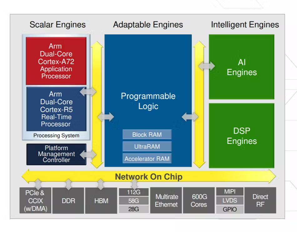
Today, it's very common to pair an FPGA with a processing system (Application Processing Unit [APU] and Real-time Processing Unit [RPU]) on a single System-on-Chip (SoC). This combination allows for low-latency communication between the on-chip Processing System (PS) and Programmable Logic (PL), enabling significant software processing capabilities alongside hardware acceleration - an all-in-one solution.
While FPGAs are capable of handling computationally intensive tasks, they generally aren't doing heavy lifting in this area - GPUs and CPUs will outperform them in most cases. Where FPGAs excel is in complex pipeline situations that work in real-time, such as automotive self-driving applications involving image capture, video processing, inference etc.
To summarize, FPGAs are particularly suited for applications that meet one or more of the following requirements:
- Low Latency Requirements - Applications that demand fast response times and minimal processing delays, such as high frequency trading systems or real-time signal processing.
- Parallel Processing Capabilities - Tasks that can be broken down into multiple concurrent operations, allowing the FPGA to process multiple data streams simultaneously for improved performance.
- Multiple Hardware Interfaces - Systems that need to communicate with various hardware components using different protocols, where the FPGA can act as a flexible interface controller handling multiple communication standards.
- Hardware Prototyping - Development scenarios where testing and validation of hardware designs are required before committing to costly ASIC fabrication, allowing for rapid iteration and verification of designs.
FPGA Architecture
To understand how FPGAs achieve their functionality, you need to have an understanding of the building blocks that make up the FPGA:
CLB (Configurable Logic Blocks)
The building blocks of FPGAs are CLBs, which can vary in architecture between different FPGA families. CLBs contain the following key components:
- Flip-Flops - A flip-flop is a fundamental sequential circuit element used to store and synchronize digital states. It captures and holds a binary value (0 or 1) at specific clock edges, maintaining that value until the next triggering clock edge occurs. Flip-flops are essential building blocks in digital design, used for synchronizing logic operations and preserving state information between clock cycles.
- Lookup Tables (LUTs) - A LUT is a fundamental building block in FPGAs that implements combinational logic by defining output values for every possible input combination. It functions like a truth table implemented in hardware, where each input combination maps to a pre-configured output value. LUTs can be programmed to implement any logical function within their input size constraints (typically 4-6 inputs in modern FPGAs).
Memory
BRAM is used to store large amounts of data within the FPGA. It consists of dedicated memory blocks that are distinct from shift registers and other memory structures. The amount of BRAM available in a design is typically limited (ranging from a few hundred kilobits in small FPGAs to around 100 megabits in large devices), so it needs to be allocated efficiently by the designer.
Digital Signal Processing (DSP) Blocks
DSP blocks are ideal for high-speed mathematical calculations. You'll find them extremely useful in digital signal processing, communications, image processing, control systems, and machine learning.
IO Blocks
IO blocks are specialized components in FPGAs that handle the communication between the internal logic fabric and external peripherals or systems. They act as the interface between the configurable logic inside the FPGA and the non-configurable parts such as pins, pads, or SerDes (Serializer/Deserializer) transceivers, and controllers.
Design Entry
Comprehensive IDEs like AMD Vivado (for AMD-based FPGAs) provide an end-to-end solution for a complete design. The IDE's capabilities encompass several key steps in the FPGA design process. First, it synthesizes the design into a gate-level representation, also known as a netlist, which represents the design using the FPGA's fundamental building blocks mentioned above. Next, the tool employs place and route algorithms to map the netlist onto the FPGA fabric efficiently. These algorithms aim to optimize resource utilization and ensure that the design meets the timing requirements specific to the chosen FPGA part.
There are two main ways to create a design on an FPGA: the traditional version using HDLs (Hardware Description Languages) like VHDL and SystemVerilog, or a graphical user interface tool that allows for plug-and-play of IP blocks from the Vivado IP catalog to create a block design. The IP integrator (IPI) route typically allows for an easier bring-up with intelligent auto-connection of key IP interfaces and devices and platform-aware dev environment, whereas the traditional RTL (Register-Transfer Level) route typically allows for greater freedom and customizability.
Below is an example of some RTL source code, it's an implementation of a simple synchronous counter with enable and reset in SystemVerilog:
module counter #(
    parameter WIDTH = 8
)(
    input  logic          clk,     // Clock input
    input  logic          rst_n,   // Active-low reset
    input  logic          en,      // Counter enable
    output logic [WIDTH-1:0] count // Counter value
);

    always_ff @(posedge clk or negedge rst_n) begin
        if (!rst_n)
            count <= '0;
        else if (en)
            count <= count + 1'b1;
    end

endmodule
The features of the IDE will vary slightly depending on the provider (Vivado for AMD devices, Quartus for Intel devices). However, each tool will typically follow the same key steps:
- Synthesis - In this step the IDE synthesizes the HDL code into a netlist, which represents the design using generic logic components. The netlist contains information about the general logic blocks being used and how they are interconnected.
- Place and Route - Firstly, the placing process maps the generic components from the synthesized netlist to the physical primitives found in your specific FPGA device. Secondly, the routing process establishes the connections between these primitives using the FPGA's physical routing resources and constraints. The tools also take into account timing constraints during this step, considering the well-defined delays of the primitives themselves.
- Bitstream Generation - Finally, the IDE generates a programmable bitstream that can be loaded onto the FPGA, configuring it to implement the desired functionality.
Large FPGA designs can have relatively long build times. When timing requirements cannot be met initially, the tools will automatically try different placement strategies and optimization algorithms. This iterative process can extend build times from hours to potentially days for designs with high resource utilization %.
How to Get Started?
Generally, having physical board access is not required to get started with FPGAs. Modern development tools allow you to create, simulate, and verify designs by targeting specific FPGA boards or part numbers. The toolchain will have all the information about the devices such as, the necessary pinouts, board files, and constraints which are needed to complete a design and close timing, however a physical board is often required for deployment and debugging.
Once you decide to run your design on hardware, there are a few accessible options. For physical hardware, I would recommend the AMD Basys 3 board. The board includes complete ready-to-use hardware, a large collection of on-board I/O devices, all required FPGA support circuits, and a free version of development tools at a student-level price point (~$150). Another option is the AWS F1 instances, where you can access a wider range of boards on a pay-per-use basis.